
- esmo semicon
- »
- contacting
contacting solutions
for demanding semiconductor test applications
Contacting expertise for complete test environments
With its dedicated Contacting Team, esmo semicon supports customers with long-standing expertise in contacting for semiconductor testing.
Drawing on several decades of combined experience in semiconductor test environments, the team complements esmo semicon’s existing activities
in handling and automation systems, test-head manipulation, docking and interface systems, and the integration of equipment into complete test cells.
Contacting is at the core of semiconductor testing. It provides the interface through which electrical signals and power are transferred between the device under test and the test system. At the same time, the mechanical conditions of the contact must remain controlled and repeatable throughout the test process.
A contacting solution needs to be matched to the complete test setup, including the device, package, electrical requirements, temperature conditions and mechanical interface. Depending on the application, key considerations can include:
- signal and power transfer
- current-carrying capability
- contact resistance stability
- high-frequency signal integrity
- temperature handling
- repeatability across test cycles

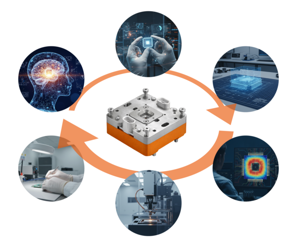
esmo semicon therefore considers contacting as part of the complete test environment rather than as an isolated component.
By combining contacting expertise with its activities in handling, automation, test-head manipulation, docking and interface systems,
esmo semicon supports customers in addressing contacting requirements within the wider test environment.
Märkte und Anwendungen
Die Anforderungen an das Contacting unterscheiden sich je nach Halbleitermarkt.
Das esmo Contacting-Team unterstützt Kunden in den folgenden relevanten Märkten und Anwendungsbereichen:
Automotive power and electric mobility
For power semiconductors used in electric vehicles, vehicle power systems and related automotive applications.
Typical focus areas include:
- electrical load and power transfer
- thermal test conditions
- package and interface design
- repeatable test behaviour
Renewable energy and grid technology
For devices used in solar inverters, wind-energy systems, energy storage and other power-conversion applications.
Typical focus areas include:
- current handling
- temperature conditions
- stable electrical interfaces
- integration into the overall test environment
Industrial automation and motor control
For semiconductors used in motor drives, robotics, factory automation and industrial control systems.
Typical focus areas include:
- power handling
- production test suitability
- mechanical stability
- long-term contact behaviour
Microcontrollers and ASICs
For digital devices used in automotive, industrial and embedded applications.
Typical focus areas include:
- parallel testing
- package geometry and interface definition
- signal integrity
- repeatable contact behaviour
Consumer electronics and embedded devices
For semiconductor devices used in consumer and connected products.
Typical focus areas include:
- compact package interfaces
- efficient test processes
- reliable electrical connections
- adaptation to the test setup
Precision analog, sensor and RF applications
For sensors, signal-conditioning devices, precision analog components and high-frequency devices.
Typical focus areas include:
- measurement stability
- controlled electrical characteristics
- signal integrity
- grounding and interface design
The applicable contacting approach depends on the individual device, package, electrical and thermal test conditions, and the architecture of the complete test environment. The required scope is defined according to the specific application and its mechanical, electrical and system interfaces.
esmo semicon is continuously expanding its Contacting activities and further developing its solutions in line with customer and application requirements. Additional information about the team’s activities and planned solutions will be added as the portfolio evolves.

Meet the Contacting Team at industry events
Visitors can meet the esmo Contacting Team live:
- at SEMICON India, taking place from 17–18 September 2026 at Yashobhoomi in Delhi, India, and
- at SEMICON Europa in Munich from 10–13 November 2026 at Messe München.
The team will be available to discuss contacting requirements, application conditions and possible approaches for semiconductor testing. Visitors are invited to discuss their device, package and test-interface requirements directly with the Contacting Team.
Talk to our Contacting experts